RF-star RF-WM-3235B1S CC3235 2.4 GHz and 5 GHz dual-band wifi module
RF-WM-3235B1S is an RF module based on TI lower-power SoC CC3235S with built-in dual-band Wi-Fi connectivity. It integrates a 40 MHz crystal, 32.768 kHz RTC clock, RF filters, diplexer, and two physical separated on-chip MCUs: Arm? Cortex?-M4 MCU with a user-dedicated 256 KB of RAM, an external plug-in 4 MB Flash, network processor for running Wi-Fi and Internet logical layers. It features 802.11 a/b/g/n: 2.4 GHz and 5 GHz support, 2.4 GHz Coexistence with Bluetooth low energy radio, improved fast scan, hostless mode for offloading template packet transmissions and application features of small size, robust connection distance, and rigid reliability.
Parameters of RF-WM-3235B1S
Chipset | CC3235S |
Supply Power Voltage | 2.7 V ~ 3.6 V, 3.3 V is recommended |
Frequency | 2.4 GHz, 5 GHz |
Transmit Power | +18.0 dBm @ 2.4 GHz (1 DSSS) +18.1 dBm @ 5 GHz (6 OFDM) |
Receiving Sensitivity | -96 dBm @ 2.4 GHz (1 DSSS) -92 dBm @ 5 GHz (6 OFDM) |
GPIO | 27 |
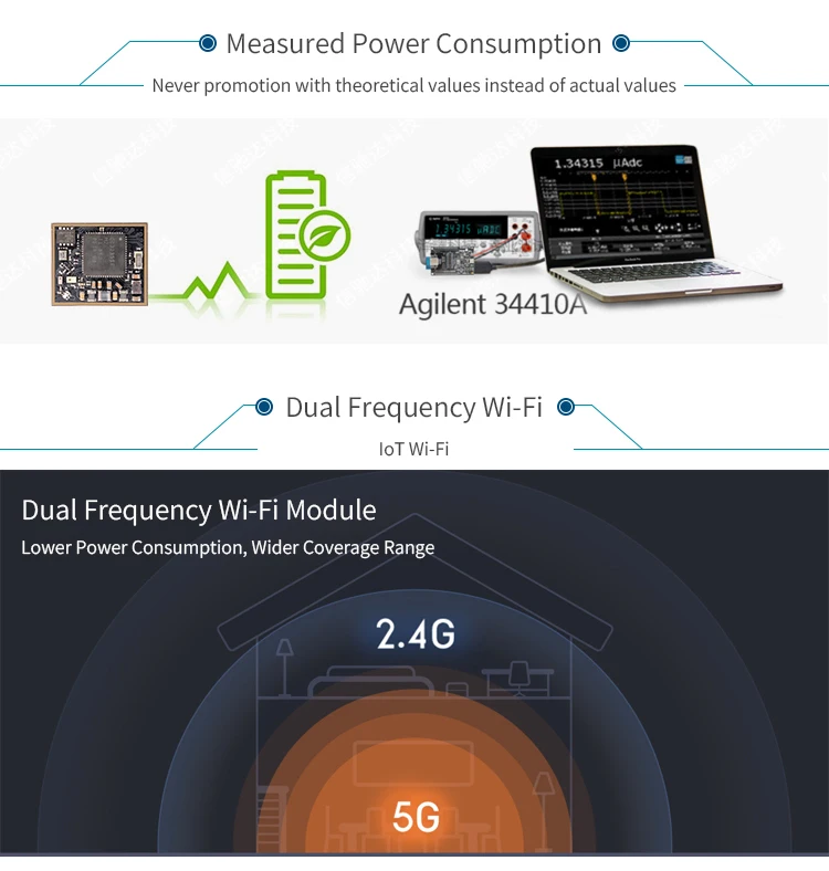
Power Consumption | Shutdown: 1 μA, hibernate: 4.5 μA Low-power deep sleep (LPDS): 120 μA Idle connected (MCU in LPDS): 710 μA RX traffic (MCU active): 59 mA TX traffic (MCU active): 223 mA |
Crystal | 40 MHz |
Package | LGA packaging |
Communication Interface | UART, I2S, I2C, SPI, SD, ADC |
Dimension | 20.5 mm × 17.5 mm |
Operating Temperature | -40 ℃~ +85 ℃ |
Storage Temperature | -55℃~ +125 ℃ |


Recommended Footprint

Pin Attributes

Pin Functions of RF-WM-3235B1S
Pin | Name | Function | Description |
1 | GND | GND | Ground |
2 | GND | GND | Ground |
3 | GPIO10 | GPIO | GPIO |
4 | GPIO11 | GPIO | GPIO |
5 | GPIO14 | GPIO | GPIO |
6 | GPIO15 | GPIO | GPIO |
7 | GPIO16 | GPIO | GPIO |
8 | GPIO17 | GPIO | GPIO |
9 | GPIO12 | GPIO | GPIO |
10 | GPIO13 | GPIO | GPIO |
11 | GPIO22 | GPIO | GPIO |
12 | JTAG-_TDI | TDI | JTAG interface: data input |
13 | FLASH_MISO | I | Serial flash interface: SPI data in |
14 | FLASH_CSN | CS | Serial flash interface: SPI chip select |
15 | FLASH_CLK | CLK | Serial flash interface: SPI clock |
16 | GND | GND | Ground |
17 | FLASH_MOSI | O | Serial flash interface: SPI data out |
18 | JTAG_TDO | TDO | JTAG interface: data output |
19 | GPIO28 | GPIO | GPIO |
20 | NC | / | No Connect |
21 | JTAG_TCK | TCK | JTAG interface: clock |
22 | JTAG_TMS | TMS | JTAG interface: mode select |
23 | SOP2 | SOP | Configuration sense-on-power |
24 | SOP1 | SOP | Configuration sense-on-power and 5 GHz switch control |
25 | GND | GND | Ground |
26 | GND | GND | Ground |
27 | GND | GND | Ground |
28 | GND | GND | Ground |
29 | GND | GND | Ground |
30 | GND | GND | Ground |
31 | RF_ABG | RF Out | RF BG band: 2.4 GHz TX, RX RF BG band: 5 GHz TX, RX |
32 | GND | GND | Ground |
33 | NC | / | No Connect |
34 | SOP0 | SOP | Configuration sense-on-power and 5 GHz switch control |
35 | NRESET | RESET | Master chip reset input. Active low input. |
36 | VBAT_RESET | RESET | VBAT reset input. Active low input. |
37 | VBAT1 | Power | Power Supply: 2.7 V ~ 3.6 V, recommend to 3.3 V |
38 | GND | GND | Ground |
39 | NC | / | No Connect |
40 | VBAT2 | Power | Power Supply |
41 | NC | / | No Connect |
42 | GPIO30 | GPIO | GPIO |
43 | GND | GND | Ground |
44 | GPIO0 | GPIO | GPIO |
45 | NC | / | No Connect |
46 | GPIO1 | GPIO | GPIO |
47 | GPIO2 | GPIO | Analog input (1.5 V max.) or GPIO |
48 | GPIO3 | GPIO | Analog input (1.5 V max.) or GPIO |
49 | GPIO4 | GPIO | Analog input (1.5 V max.) or GPIO |
50 | GPIO5 | GPIO | Analog input (1.5 V max.) or GPIO |
51 | GPIO6 | GPIO | GPIO |
52 | GPIO7 | GPIO | GPIO |
53 | GPIO8 | GPIO | GPIO |
54 | GPIO9 | GPIO | GPIO |
55 | GND | / | Thermal ground |
56 | GND | / | Thermal ground |
57 | GND | / | Thermal ground |
58 | GND | / | Thermal ground |
59 | GND | / | Thermal ground |
60 | GND | / | Thermal ground |
61 | GND | / | Thermal ground |
62 | GND | / | Thermal ground |
63 | GND | / | Thermal ground |


