TI CC3220SF Long range ultra-low power consumption RF-WM-3220B1 2.4GHz Wi-Fi Module
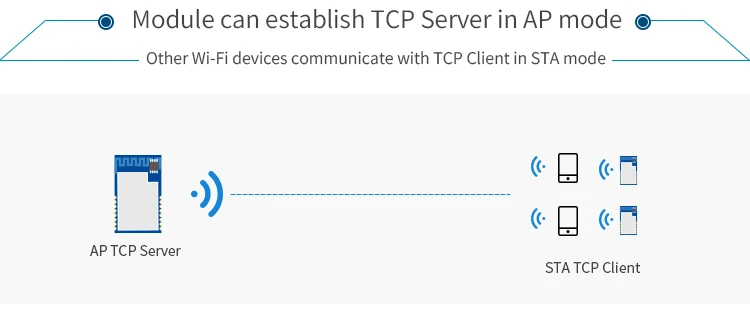
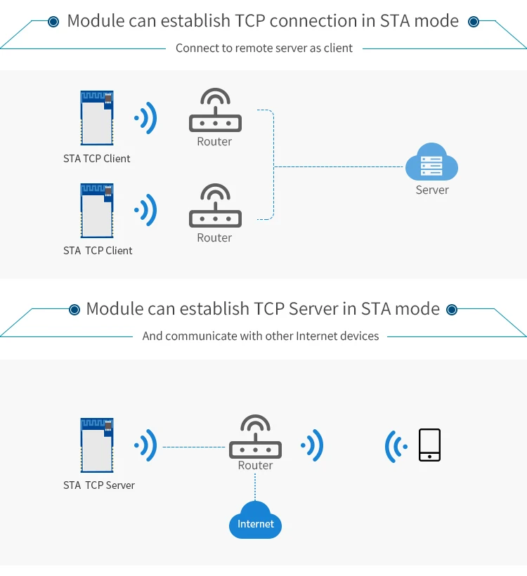
RF-WM-3220B1 series is a low power Wi-Fi SoC module which is based on TI SimpleLinkTM Wi-Fi? SoC CC3220S / CC3220R / CC3220SF, which has a built-in ARM CortexTM-M4 core processor with a user-dedicated 256 KB of RAM and an optional 1 MB of serial flash, a network processor MCU runs all Wi-Fi? and internet logical layers, and a variety of peripherals including parallel camera interface, I2S, SD/MMC, UART, SPI, I2C, ADC and GPIOs. The ROM-based subsystem of RF-WM-3220B1 includes an IEEE 802.11 b/g/n radio, baseband, and MAC with a powerful crypto engine. The module supports station, access point with support of four stations, and Wi-Fi Direct? modes. The device also supports WPA2 personal and enterprise security and WPS 2.0. The Wi-Fi Internet-on-a-chip includes embedded IPv4 and IPv6 TCP/IP protocols. The power-management subsystem includes integrated DC-DC converters supporting a wide range of supply voltages. This subsystem enables low-power consumption modes, such as the hibernate with RTC mode requiring less than 4.5 μA of current. The module design provides 3 options for antenna integration, including surface mounted chip antenna, an IPEX interface for connecting an external antenna, and a RF pad for soldering onto the base board and routing to an on-board antenna. RF-WM-3220B1 series is pin-2-pin compatible with RF-WM-3200B1.
Function Difference of RF-WM-3220B1 Series Module
Model | Chipset | Functions of Chipset |
RF-WM-3220RB1 | CC3220R | 256 KB of RAM, IoT networking security and device identity/keys. |
RF-WM-3220SB1 | CC3220S | Builds on the CC3220R and with enhanced application level security, secure boot. |
RF-WM-3220B1 | CC3220SF | Builds on the CC3220R and with enhanced application level security, secure boot, 1 MB of executable flash. |
Parameters of RF-WM-3220B1
Chipset | CC3220SF |
Supply Power Voltage | 2.7 V ~ 3.6 V, 3.3 V is recommended |
Frequency | 2.4 GHz |
Working Mode | 802.11 b/g/n station, 802.11 b/g/n access point with support of 4 stations, Wi-Fi Direct?Client and Group Owner |
Transmit Power | +18.0 dBm @ 1 DSSS +14.5 dBm @ 54 OFDM |
Receiving Sensitivity | -95.7 dBm @ 1 DSSS -74.0 dBm @ 54 OFDM |
GPIO | 29 |
Power Consumption | Shutdown: 1 μA Hibernate: 4.5 μA Low-power deep sleep (LPDS): 135 μA Idle connected (MCU in LPDS): 710 μA @ DTIM = 1 RX traffic (MCU active): 59 mA @ 54 OFDM TX traffic (MCU active): 223 mA @ 54 OFDM, maximum power |
Crystal | 40 MHz, 32.768 kHz |
Package | SMT packaging, half-hole packaging |
Communication Interface | UART, I2S, I2C, SPI, SD/MMC, ADC, DMA, PWM, McASP, Camera interface |
Dimension | 31.0 mm × 20.0 mm |
Operating Temperature | -30 ℃~ +85 ℃ |
Storage Temperature | -55℃~ +125 ℃ |


Recommended Footprint

Pin Attributes

Pin Functions of RF-WM-3220B1 Series
Pin | Chip Pin | Name | Function |
1 |
| GND | Ground |
2 |
| RF_OUT | RF output interface |
3 | 50 | GPIO00 | GPIO0 |
UART0_CTS |
McAXR1 |
GT_CCP00 |
GSPI_CS |
UART1_RTS |
UART0_RTS |
McAXR0 |
4 | 53 | GPIO30 | GPIO30 |
UART0_TX |
McACLK |
McAFSX |
GT_CCP05 |
GSPI_MISO |
5 | 55 | GPIO01 | GPIO1 |
UART0_TX |
pCLK Pixel (PIXCLK) |
UART1_TX |
GT_CCP01 |
6 | 57 | GPIO02 | ADC_CH0 |
GPIO2 |
UART0_RX |
UART1_RX |
GT_CCP02 |
7 | 58 | GPIO03 | ADC_CH1 |
GPIO3 |
UART1_TX |
pDATA7(CAM_D3) |
8 | 59 | GPIO04 | ADC_CH2 |
GPIO4 |
UART1_RX |
pDATA6 (CAM_D2) |
9 | 60 | GPIO05 | ADC_CH3 |
GPIO5 |
pDATA5 (CAM_D1) |
McAXR1 |
GT_CCP05 |
10 | 61 | GPIO06 | GPIO6 |
UART0_RTS |
pDATA4 (CAM_D0) |
UART1_CTS |
UART0_CTS |
GT_CCP06 |
11 | 62 | GPIO07 | GPIO7 |
McACLKX |
UART1_RTS |
UART0_RTS |
UART0_TX |
12 | 63 | GPIO08 | GPIO8 |
SDCARD_IRQ |
McAFSX |
GT_CCP06 |
13 | 64 | GPIO09 | GPIO9 |
GT_PWM05 |
SDCARD_DATA0 |
McAXR0 |
GT_CCP00 |
14 | 1 | GPIO10 | GPIO10 |
I2C_SCL |
GT_PWM06 |
UART1_TX |
SDCARD_CLK |
GT_CCP01 |
15 | 2 | GPIO11 | GPIO11 |
I2C_SDA |
GT_PWM07 |
pXCLK(XVCLK) |
SDCARD_CMD |
UART1_RX |
GT_CCP02 |
McAFSX |
16 | 3 | GPIO12 | GPIO12 |
McACLK |
pVS (VSYNC) |
I2C_SCL |
UART0_TX |
GT_CCP03 |
17 | 4 | GPIO13 | GPIO13 |
I2C_SDA |
pHS (HSYNC) |
UART0_RX |
GT_CCP04 |
18 | 5 | GPIO14 | GPIO14 |
I2C_SCL |
GSPI_CLK |
pDATA8 (CAM_D4) |
GT_CCP05 |
19 | 6 | GPIO15 | GPIO15 |
I2C_SDA |
GSPI_MISO |
pDATA9(CAM_D5) |
GT_CCP06 |
SDCARD_DATA0 |
20 | 7 | GPIO16 | GPIO16 |
GSPI_MOSI |
pDATA10 (CAM_D6) |
UART1_TX |
GT_CCP07 |
SDCARD_CLK |
21 | 8 | GPIO17 | GPIO17 |
UART1_RX |
GSPI_CS |
pDATA11 (CAM_D7) |
SDCARD_CMD |
22 | 15 | GPIO22 | GPIO22 |
McAFSX |
GT_CCP04 |
23 | 16 | JTAG TDI | TDI |
GPIO23 |
UART1_TX |
I2C_SCL |
24 | 17 | JTAG TDO | TDO |
GPIO24 |
PWM0 |
UART1_RX |
I2C_SDA |
GT_CCP06 |
McAFSX |
25 | 18 | GPIO28 | GPIO28 |
26 | 19 | JTAG TCK | TCK |
GT_PWM03 |
27 | 20 | JTAG TMS | TMS |
GPIO29 |
28 | 29 | ANTSEL1 | I/O |
29 | 30 | ANTSEL2 | I/O |
30 | 32 | RESET | Module reset pin, internal pull-up by default, active low |
31 | 45 | DCDC_ANA2 | GPIO31 |
UART0_RX |
McAFSX |
UART1_RX |
McAXR0 |
GSPI_CLK |
DCDC_ANA2_SW_P |
32 | 35 | SOP0 | SOP0 |
33 | 34 | SOP1 | SOP1 |
34 | 21 | SOP2 | GPIO25 |
GT_PWM02 |
McAFSX |
TCXO_EN |
SOP2 |
35 |
| VCC | Power supply, 2.3 V ~ 3.6 V |
36 |
| GND | Ground |


